- 您现在的位置:买卖IC网 > Sheet目录369 > W9864G6JH-6I (Winbond Electronics)IC SDRAM 64MBIT 54TSOPII
�� �
�
�W9864G6JH�
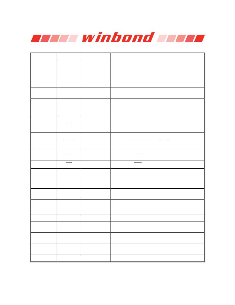
�5.� PIN� DESCRIPTION�
�PIN� NUMBER�
�PIN� NAME�
�FUNCTION�
�DESCRIPTION�
�Multiplexed� pins� for� row� and� column� address.�
�23� ~� 26,� 22,�
�29� ~35�
�A0� ?� A11�
�Address�
�Row� address:� A0� ?� A11.� Column� address:� A0� ?� A7.�
�A10� is� sampled� during� a� precharge� command� to�
�determine� if� all� banks� are� to� be� precharged� or� bank�
�selected� by� BS0,� BS1.�
�20,� 21�
�2,� 4,� 5,� 7,� 8,� 10,�
�11,� 13,� 42,� 44,�
�45,� 47,� 48,� 50,�
�51,� 53�
�BS0,� BS1�
�DQ0� ?� DQ15�
�Bank� Select�
�Data�
�Input/� Output�
�Select� bank� to� activate� during� row� address� latch� time,�
�or� bank� to� read/write� during� address� latch� time.�
�Multiplexed� pins� for� data� output� and� input.�
�Disable� or� enable� the� command� decoder.� When�
�19�
�CS�
�Chip� Select�
�command� decoder� is� disabled,� new� command� is�
�ignored� and� previous� operation� continues.�
�18�
�RAS�
�Row� Address�
�Strobe�
�Command� input.� When� sampled� at� the� rising� edge� of�
�the� clock� RAS� ,� CAS� and� WE� define� the�
�operation� to� be� executed.�
�17�
�CAS�
�Column�
�Address� Strobe� Referred� to� RAS�
�16�
�39,� 15�
�38�
�WE�
�UDQM�
�LDQM�
�CLK�
�Write� Enable�
�Input/output�
�mask�
�Clock� Inputs�
�Referred� to� RAS�
�The� output� buffer� is� placed� at� Hi-Z� (with� latency� of� 2)�
�when� DQM� is� sampled� high� in� read� cycle.� In� write�
�cycle,� sampling� DQM� high� will� block� the� write�
�operation� with� zero� latency.�
�System� clock� used� to� sample� inputs� on� the� rising�
�edge� of� clock.�
�CKE� controls� the� clock� activation� and� deactivation.�
�37�
�CKE�
�Clock� Enable�
�When� CKE� is� low,� Power� Down� mode,� Suspend�
�mode,� or� Self� Refresh� mode� is� entered.�
�1,� 14,� 27�
�28,� 41,� 54�
�3,� 9,� 43,� 49�
�6,� 12,� 46,� 52�
�V� DD�
�V� SS�
�V� DDQ�
�V� SSQ�
�Power�
�Ground�
�Power� for� I/O�
�buffer�
�Ground� for� I/O�
�buffer�
�Power for input buffers and logic circuit inside DRAM.�
�Ground� for� input� buffers� and� logic� circuit� inside�
�DRAM.�
�Separated� power� from� V� DD� ,� to� improve� DQ� noise�
�immunity.�
�Separated� ground� from� V� SS� ,� to� improve� DQ� noise�
�immunity.�
�36,� 40�
�NC�
�No� Connection� No� connection.�
�-5-�
�Publication� Release� Date:� Jun.� 25,� 2013�
�Revision� A04�
�发布紧急采购,3分钟左右您将得到回复。
相关PDF资料
WM-5614
CABINET WALL MOUNT 37.25X17.9"
WRR-2244
RACK WALL MOUNT RELAY 42" X 19"
WRR-2264
RACK WALL MOUNT 75.25" X 19"
X28C512JIZ-12
IC EEPROM 512KBIT 120NS 32PLCC
X28HC256SIZ-90
IC EEPROM 256KBIT 90NS 28SOIC
X28HC64JIZ-90
IC EEPROM 64KBIT 90NS 32PLCC
XCARD XK-1A
DEV KIT EVENT-DRIVEN PROC XS1-L1
XCARD XTAG-2
ADAPTER USB DEBUGGER JTAG XSYS2
相关代理商/技术参数
W9864G6JH-6I/TRAY
制造商:Winbond Electronics Corp 功能描述:
W9864G6JH-7
制造商:WINBOND 制造商全称:Winbond 功能描述:Self Refresh Current: Standard and Low Power, Sequential and Interleave Burst
W9864G6JH-7S
制造商:WINBOND 制造商全称:Winbond 功能描述:Self Refresh Current: Standard and Low Power, Sequential and Interleave Burst
W9864G6JT
制造商:WINBOND 制造商全称:Winbond 功能描述:1M ? 4 BANKS ? 16 BITS SDRAM
W9864G6JT-6
制造商:Winbond Electronics Corp 功能描述:IC SDRAM 64MBIT 166MHZ 制造商:Winbond Electronics Corp 功能描述:IC SDRAM 64MBIT 166MHZ 54TFBGA
W987D2HB
制造商:WINBOND 制造商全称:Winbond 功能描述:128Mb Mobile LPSDR
W987D2HBGX6E
制造商:WINBOND 制造商全称:Winbond 功能描述:128Mb Mobile LPSDR
W987D2HBGX6I
制造商:WINBOND 制造商全称:Winbond 功能描述:128Mb Mobile LPSDR