- 您现在的位置:买卖IC网 > Sheet目录369 > W9864G6JH-6I (Winbond Electronics)IC SDRAM 64MBIT 54TSOPII
W9864G6JH
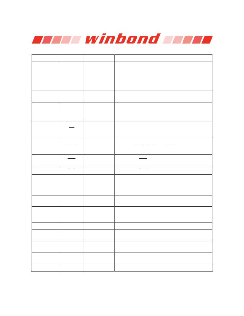
5. PIN DESCRIPTION
PIN NUMBER
PIN NAME
FUNCTION
DESCRIPTION
Multiplexed pins for row and column address.
23 ~ 26, 22,
29 ~35
A0 ? A11
Address
Row address: A0 ? A11. Column address: A0 ? A7.
A10 is sampled during a precharge command to
determine if all banks are to be precharged or bank
selected by BS0, BS1.
20, 21
2, 4, 5, 7, 8, 10,
11, 13, 42, 44,
45, 47, 48, 50,
51, 53
BS0, BS1
DQ0 ? DQ15
Bank Select
Data
Input/ Output
Select bank to activate during row address latch time,
or bank to read/write during address latch time.
Multiplexed pins for data output and input.
Disable or enable the command decoder. When
19
CS
Chip Select
command decoder is disabled, new command is
ignored and previous operation continues.
18
RAS
Row Address
Strobe
Command input. When sampled at the rising edge of
the clock RAS , CAS and WE define the
operation to be executed.
17
CAS
Column
Address Strobe Referred to RAS
16
39, 15
38
WE
UDQM
LDQM
CLK
Write Enable
Input/output
mask
Clock Inputs
Referred to RAS
The output buffer is placed at Hi-Z (with latency of 2)
when DQM is sampled high in read cycle. In write
cycle, sampling DQM high will block the write
operation with zero latency.
System clock used to sample inputs on the rising
edge of clock.
CKE controls the clock activation and deactivation.
37
CKE
Clock Enable
When CKE is low, Power Down mode, Suspend
mode, or Self Refresh mode is entered.
1, 14, 27
28, 41, 54
3, 9, 43, 49
6, 12, 46, 52
V DD
V SS
V DDQ
V SSQ
Power
Ground
Power for I/O
buffer
Ground for I/O
buffer
Power for input buffers and logic circuit inside DRAM.
Ground for input buffers and logic circuit inside
DRAM.
Separated power from V DD , to improve DQ noise
immunity.
Separated ground from V SS , to improve DQ noise
immunity.
36, 40
NC
No Connection No connection.
-5-
Publication Release Date: Jun. 25, 2013
Revision A04
发布紧急采购,3分钟左右您将得到回复。
相关PDF资料
WM-5614
CABINET WALL MOUNT 37.25X17.9"
WRR-2244
RACK WALL MOUNT RELAY 42" X 19"
WRR-2264
RACK WALL MOUNT 75.25" X 19"
X28C512JIZ-12
IC EEPROM 512KBIT 120NS 32PLCC
X28HC256SIZ-90
IC EEPROM 256KBIT 90NS 28SOIC
X28HC64JIZ-90
IC EEPROM 64KBIT 90NS 32PLCC
XCARD XK-1A
DEV KIT EVENT-DRIVEN PROC XS1-L1
XCARD XTAG-2
ADAPTER USB DEBUGGER JTAG XSYS2
相关代理商/技术参数
W9864G6JH-6I/TRAY
制造商:Winbond Electronics Corp 功能描述:
W9864G6JH-7
制造商:WINBOND 制造商全称:Winbond 功能描述:Self Refresh Current: Standard and Low Power, Sequential and Interleave Burst
W9864G6JH-7S
制造商:WINBOND 制造商全称:Winbond 功能描述:Self Refresh Current: Standard and Low Power, Sequential and Interleave Burst
W9864G6JT
制造商:WINBOND 制造商全称:Winbond 功能描述:1M ? 4 BANKS ? 16 BITS SDRAM
W9864G6JT-6
制造商:Winbond Electronics Corp 功能描述:IC SDRAM 64MBIT 166MHZ 制造商:Winbond Electronics Corp 功能描述:IC SDRAM 64MBIT 166MHZ 54TFBGA
W987D2HB
制造商:WINBOND 制造商全称:Winbond 功能描述:128Mb Mobile LPSDR
W987D2HBGX6E
制造商:WINBOND 制造商全称:Winbond 功能描述:128Mb Mobile LPSDR
W987D2HBGX6I
制造商:WINBOND 制造商全称:Winbond 功能描述:128Mb Mobile LPSDR
